
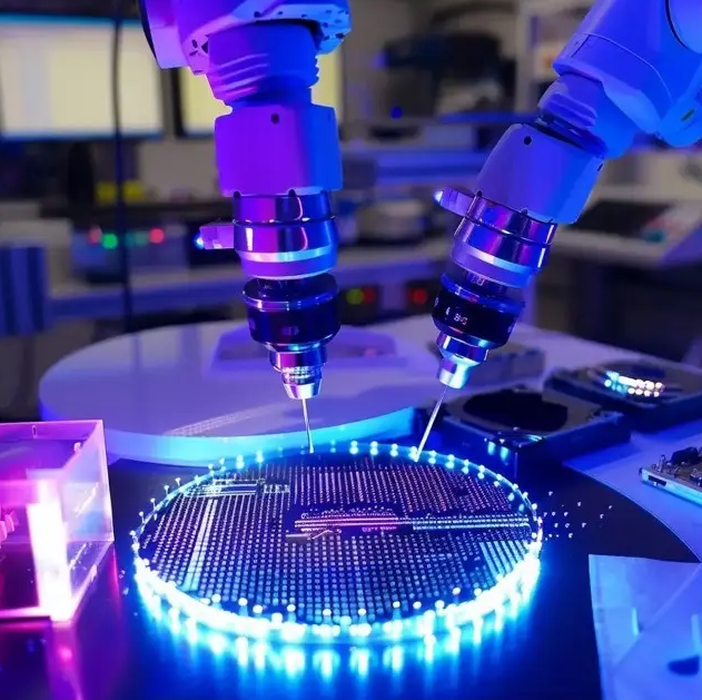
On the fab floor, smart sensor packaging lines can’t tolerate thermal drift. One soft bake that drifts out of spec, one hard bake with a hot spot, and your yield starts slipping before lithography even finishes. We built an infrared thermal platform to take that variability off the table. What matters under the hood We use NIR emitters tuned to the photoresist absorption, so the heat lands fast and contactless. Across the bake zone, wafer-level uniformity holds ±0.1°C, and repeatability is nailed down with closed-loop pyrometry right at the substrate plane. The heater body is quartz and high-purity ceramic, so under steady state you’re not generating particles. It runs in Class 1–100 cleanrooms without lifting particle counts, and the thermal profile stays consistent lot to lot. Power density is managed to respect thin-film thermal budgets, and the response time keeps throughput moving—no waiting around for mass thermal settling. Why it fits smart sensor packaging You’re running thin films, delicate bumps, and an overlay budget that has no room for excuses. With this infrared bake, photoresist processing stays inside the window: soft bakes that dry evenly, hard bakes that harden without overshoot. The payoff is fewer reworks, fewer scrap wafers, and critical dimension control that behaves itself. The platform also cuts energy use by getting rid of idle-hot idling. It heats on demand and cools quickly, so your utility draw drops while cycle time stays tight. Reliability is built for 24/7, with emitter life tracked and compensated so temperature stays on spec. What you need to plan for Installation needs a clean power feed and a stable mount plane. The emitter array is sensitive to misalignment, and if you’re off, you can see a small shadowing effect at wafer edges. Run a short qualification to set the recipe, then lock the setpoints into your control plan. Once aligned, the process is repeatable—but it does demand disciplined preventive checks on optics and pyrometer calibration.