



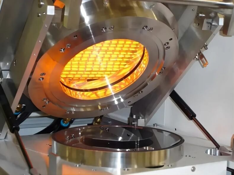
On the fab floor, a 1°C drift during the photoresist bake is enough to shift a linewidth by nanometers—and that’s a whole lot scrapped. You don’t chase temperature; you hold it. We built the OEM semiconductor heating element to lock control at the wafer, not just at the setpoint. What matters under the hood The element uses short-wave infrared (SWIR) halogen emitters in a quartz body, so ramp rates are fast and steady-state control is tight. The spec you care about is wafer-level uniformity: ±0.1°C across the active zone, measured in situ. It runs in Class 1–100 cleanrooms without adding particles, and that’s backed by in-chamber monitoring. Output repeatability stays within ±0.2% even on 24/7 duty cycles, and the thermal response is tuned specifically for photoresist soft bake and hard bake profiles. You can spec it for 200/300 mm wafers, with standard voltages and a compact footprint that fits OEM tool envelopes. Why it holds up in production In lithography and packaging lines, this element keeps bake profiles on target, so you’re not chasing rework. Tight uniformity cuts across-wafer CD error and helps yield on tight nodes. The cycles are fast and stable, which shortens time per lot, and the cleanroom-compatible design keeps particle counts down—fewer scrubs, fewer alarms. Energy use is optimized by precise emitter matching and low thermal mass, which lowers cost per wafer. When it’s time to swap, the module goes in without tearing down the process chamber, so unplanned downtime drops. What to watch for You’ll need matched sockets and proper shielding to keep stray heat off optics and polymers. There’s a warm-up period before you hit the rated uniformity—plan it into PM. For the best stability, stay within the specified voltage tolerance and keep ambient temperature controlled. We support integration with major OEM platforms, but run the pinout, mounting, and cooling paths by your equipment team before you deploy.